LTO batteries, or Lithium Titanium Oxide batteries, have one enormous advantage — they can be charged and discharged at sub-zero temperatures. This makes them ideal for applications such as weather stations, Meshtastic nodes, and other outdoor electronics.
However, the average hobbyist’s use can be a bit more complicated because they have a lower voltage than standard Li-Ion or Li-Pol batteries, and there is no available electronic protection for single-cell LTO. That’s why I set out to design my own solution that, in addition to OVLO/UVLO/OC, also continuously measures the cell parameters and communicates them over I2C. Below, you’ll find my development notes for this BMS.
A Bit of Theory
Comparison of Different Battery Types
Below is a table comparing the different chemistries of lithium cells (and for interest, the new sodium-ion chemistry as well). The values for individual parameters are indicative, as they vary greatly from manufacturer to manufacturer. However, it is sufficient for an introductory understanding of LTO.
| Parameter | Unit | Li-Ion/Li-Pol | LiFePo4 | Sodium-Ion | LTO |
|---|---|---|---|---|---|
| Min. voltage | V | 2,5 – 3,0 | 2,5 | 1,5 – 2,0 | 1,5 – 1,7 |
| Max. voltage | V | 4,2 – 4,4 | 3,65 | 3,6 – 3,8 | 2,8 – 2,9 |
| Energy density | Wh/kg | 150-250 | 90-160 | 100-160 | 70-110 |
| Operating temperature (charging) | °C | 0 – 45 | 0 – 45 | 0 – 40 | −10 – 55 |
| Operating temperature (discharging) | °C | −20 – 60 | −20 – 60 | −20 – 60 | −30 – 60 |
| Max charge rate | C | 1 – 2 | 1 – 2 | 0,5 – 1 | 5 – 10 |
| Max discharge rate | C | 1 – 10 | 10 – 25 | 1 – 5 | 10 – 20 |
| Cycle life | – | 500 – 1500 | 2000 – 5000 | 1000 – 2000 | 3000 – 7000 |
| Safety | – | Medium, electronic protection is necessary. | Very safe | Safe | Very safe |
LTO batteries have lower energy density than other types, so less Ah fits into the same package. They have a lower operating voltage, a minimum of 1.5 V (some sources and manufacturers report 1.7 V), and a maximum of 2.8 V (again, you may read 2.9 V elsewhere). They support high charging and discharging currents due to their low internal resistance. This is thanks to the titanium nanostructure inside, which has a large surface area (hundreds of m2.g-1 versus units of m2.g-1 in Li-Ion) allowing electrons to move across the anode much faster. Another great advantage is their longer lifespan, which is stated to be up to 7000 cycles.
LTO batteries are chemically very stable, posing no risks of swelling, fires, or explosions like Li-Ion or Li-Poly cells. Some manufacturers claim that LTO can be discharged to 0 V and overcharged above 3 V without exploding or getting damaged. However, such usage would shorten the lifetime of the cell and is not recommended.
And now, the most vital parameter for us: the temperature range for charging and discharging. LTO are the only lithium-based cells that can be charged at temperatures around −10°C without damaging the battery or significantly shortening its lifespan. For the temperatures in Central Europe, it’s an ideal type of battery for outdoor use.
Discharge Curve
The voltage on LTO batteries drops rapidly from 2.8 V to about 2.6 V during discharge and then decreases very slowly to 2.3 V. Once the battery is nearly discharged, the voltage plummets from 2.3 to below 1.7 V even with a small load.
With a larger load (faster discharge), the curve is similar but slightly lower (about 0.3 V lower at 1C and 0.5 V lower at 5C), and the sharp drop in the nearly discharged state begins sooner.
Why BMS for 1S LTO?
My motivation for designing my electronic protection for single-cell LTO batteries is mainly for their use in the Meshtastic project. Nodes powered by batteries and charged through a solar panel are typically placed outside, and I want them to be chargeable even in winter when the sun briefly shines. Currently, I’m using 1S Li-Pol batteries, but with winter around the corner, it’s time to look for alternatives.
Hence my needs for the BMS:
- Protection must be for 1S LTO batteries. I already have a Mesthastic board prepared for them, and such protection does not yet exist (all protections/BMS I found are from 4S LTO and bigger packs), so it makes sense to develop my own.
- Low discharge currents in the tens of mA, up to hundreds of mA.
- Charging currents up to 1 A (or to the maximum power of the solar panel).
- Protection against under-voltage (UVLO), over-voltage (OVLO), and overcurrent (OC).
- Limit or completely shut down charging/discharging at temperatures beyond the allowed working range.
- Anything extra (configuration options, measurement, etc.) would be nice but isn’t necessary.
Prototype No. 1
The first idea was to create LTO protection purely analog. I picked a suitable comparator capable of rail-to-rail output, with minimal consumption and which can handle a power supply range of at least 1.3 to 3.0 V. NCS2220A from Onsemi meets all these requirements.
Another important component is P-channel MOSFET transistors to limit current in one direction or both. After extensively combing through datasheets, I eventually settled on EV3415, as they were the best choice available at JLCPCB and in stock.
On the other hand, finding a good voltage reference that works for voltages around 1.3 V proved almost impossible. I finally chose AZ431, though it wasn’t a great choice, as I’ll explain later.

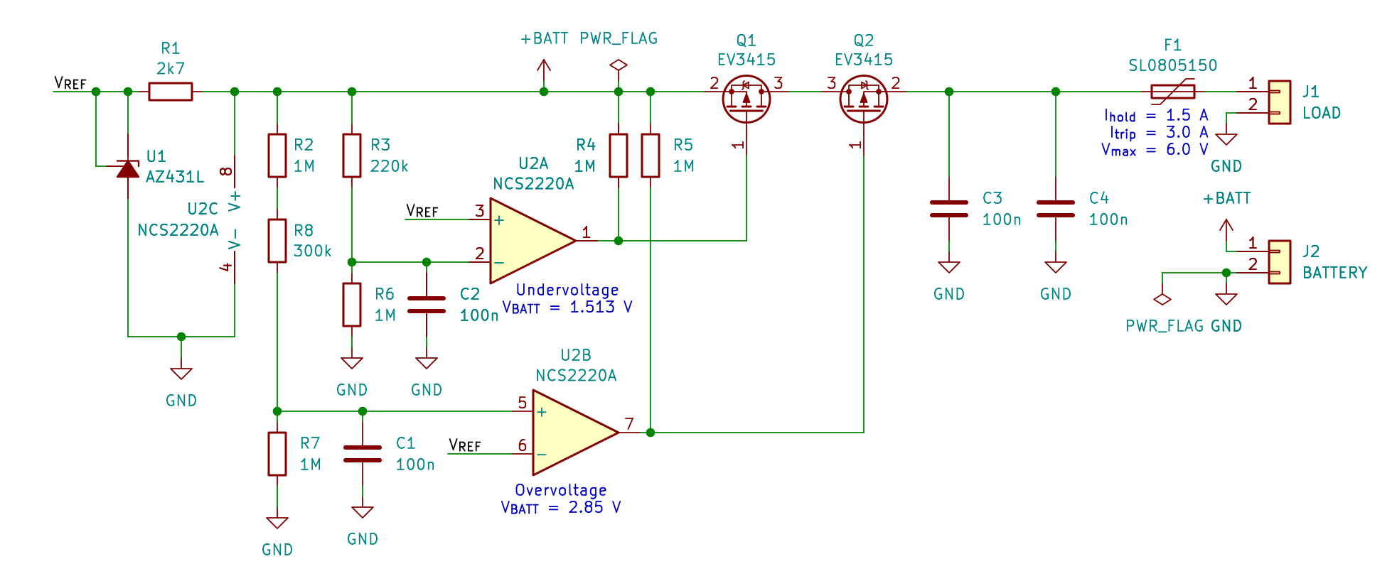
The working principle of this circuit is following:
- If the cell’s voltage is less than 1.513 V, the comparator U2A will output the supply voltage, closing Q1 and stopping the current from flowing from the battery to the load. Thanks to the body-diode Q1, current can still flow in the direction from the load to the battery, allowing the cell to keep charging. This is the UVLO or under-voltage lockout state.
- If the cell’s voltage is greater than 2.85 V, comparator U2B activates and shuts off transistor Q2. This stops the current from flowing from the load to the battery and stops charging. This is the OVLO or over-voltage lockout state.
- If the voltage is between 1.513 and 2.850 V, both comparators are inactive, the gates of both transistors are connected to GND, and therefore they are open. Current can flow in both directions.
- An overcurrent (OC) condition is protected by PPTC F1 in the circuit, which disconnects the load for currents greater than 3 A. Once the current reduces, PPTC returns to normal functionality.
- For comparators, a voltage reference is required, in this case, AZ431, which consumes too much power and unnecessarily discharges the battery.
- If either the comparator or voltage reference stops functioning for any reason, the battery will be disconnected from the load. This is the default state.
This circuit design pushed me out of my “digital” comfort zone :) At least I had a reason to refresh my knowledge. Due to the tiny UDNF8 case of comparator U2, I chose to have the first 5 prototypes assembled by JLCPCB.
Unfortunately, my efforts to become an analog wizard were not successful. While the circuit didn’t burn out and almost acted as intended, there were several issues:
- Disconnection for under-voltage works – 1.519 V @ 100 µA and 1.560 V @ 1.05 A.
- For over-voltage, disconnection does not occur even though the change is visible, indicating that the comparator works. Q2 likely opens by the S-G voltage because the charger voltage exceeds U2’s power supply.
- In both transition states (UVLO and OVLO), the circuit oscillates. This is caused by a sudden change in cell voltage when disconnecting/connecting a load or charging. The hysteresis at the comparator inputs isn’t sufficient.
- The voltage reference’s consumption is excessive. I expected as much during the schematic design, but it deserves mentioning.
I started adjusting the circuit and trying to resolve all the issues, but the entire circuit began to complicate quickly, adding more components, and eventually, I couldn’t even find a better voltage reference. In the end, I decided to abandon this approach and use a cheap and small microcontroller that would handle everything: monitoring voltage, current direction, voltage reference, and hysteresis implemented in code. All in one component for less than 1 USD.
Prototype No. 2
Only the P-channel MOSFET transistors and PPTC fuse remained, from the first prototype. Everything else changed.
The core of the design is the ATtiny824 microcontroller, which is part of the ATtiny 2-series from Microchip. This MCU family was introduced around 2022, so it’s relatively new, can be programmed via UPDI interface (as opposed to the earlier AVR SPI), comes with an internal 20 MHz crystal, low-power 32.768 kHz crystal, 12-bit multi-channel single-ended or differential ADC, RTC, UART, TWI, and more. Moreover, I have extensive experience with AVR and have worked with series-0 and series-1. ATtiny824 appears to be an ideal candidate for LTO BMS, except for one catch…
The operating voltage of this MCU is from 1.8 V (at a maximum CPU frequency of 5 MHz) to 5.5 V, but we need at least 1.3 V. It’s unacceptable for the BMS to stop functioning at a fully discharged battery (<1.5 V). If the MCU doesn’t work, transistors won’t open, and it won’t be possible to charge the battery. If left without charge for longer, the voltage may fall even further, potentially down to 1 V.
To boost the voltage for the MCU, I eventually chose a charge pump. The simple and widespread ICL7660 can be connected as a voltage doubler, requiring only 2 Schottky diodes and 4 capacitors. The pump’s oscillator oscillates at relatively low frequencies and can be slowed to ~1 kHz for loads in the mA range. This seemed advantageous compared to a boost converter with a coil and switching frequency of around 1 MHz, promising better efficiency and reduced EMI risk.


The BMS functions as follows:
- ATtiny will use an ADC voltage reference of 1.024 V. With 12 bits, this gives a resolution of 250 µV per LSB. By implementing oversampling, the accuracy can be further increased (for example, increasing accuracy by 2 bits requires 16 samples, raising precision to 62.5 µV/LSB).
ADC_BATTmonitors battery voltage through a voltage divider with a ratio of 0.3. This transforms 1.3 to 2.8 V on the cell to 0.43 – 0.93 V at the ADC input. The battery voltage can thus be monitored with a precision of 187.5 µV/LSB, more than sufficient.ADC_OUTmonitors the voltage on the load using the same voltage divider as before. Everything stated above applies.- The current to and from the cell will be measured using the ADC in differential mode through a shunt resistor of 0.1 Ω, which ranges from 100 µV to 200 mV for currents of 1 mA to 2000 mA. This results in a maximum of 0.4 W power loss on the resistor, requiring a larger SMD package. The chosen resistor is SMD1812 rated for 750 mW.
- The ADC in ATtiny contains a Programmable Gain Amplifier (PGA), which can amplify the voltage across the shunt resistor in steps of 1×, 2×, 4×, 8×, and 16× before conversion, allowing higher measurement accuracy for small currents.
- The ATtiny code will periodically measure all voltages and, based on set rules, toggle both MOSFET transistors simultaneously via the
CUTOFFsignal. - The PPTC fuse monitors overcurrent conditions and will protect the cell from a short circuit by disconnecting the load. In normal operation, where there’s no short circuit but just a slight over-current condition, the load will be disconnected by the MCU.
- Ambient temperature is measured by the internal thermistor in the MCU, connected to one of the ADC channels. The same code used for the battery voltage allows for temperature measurement. This enables disabling charging or discharging at extreme temperatures outside the allowed working range.
- The setup includes an I2C bus connection, allowing the entire BMS to be connected to an I2C master for tracking voltages, current, remaining capacity, cycle count, and more. A pleasant bonus that wasn’t possible in the previous design version.
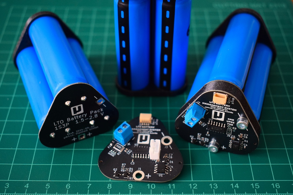
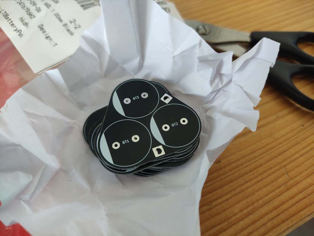
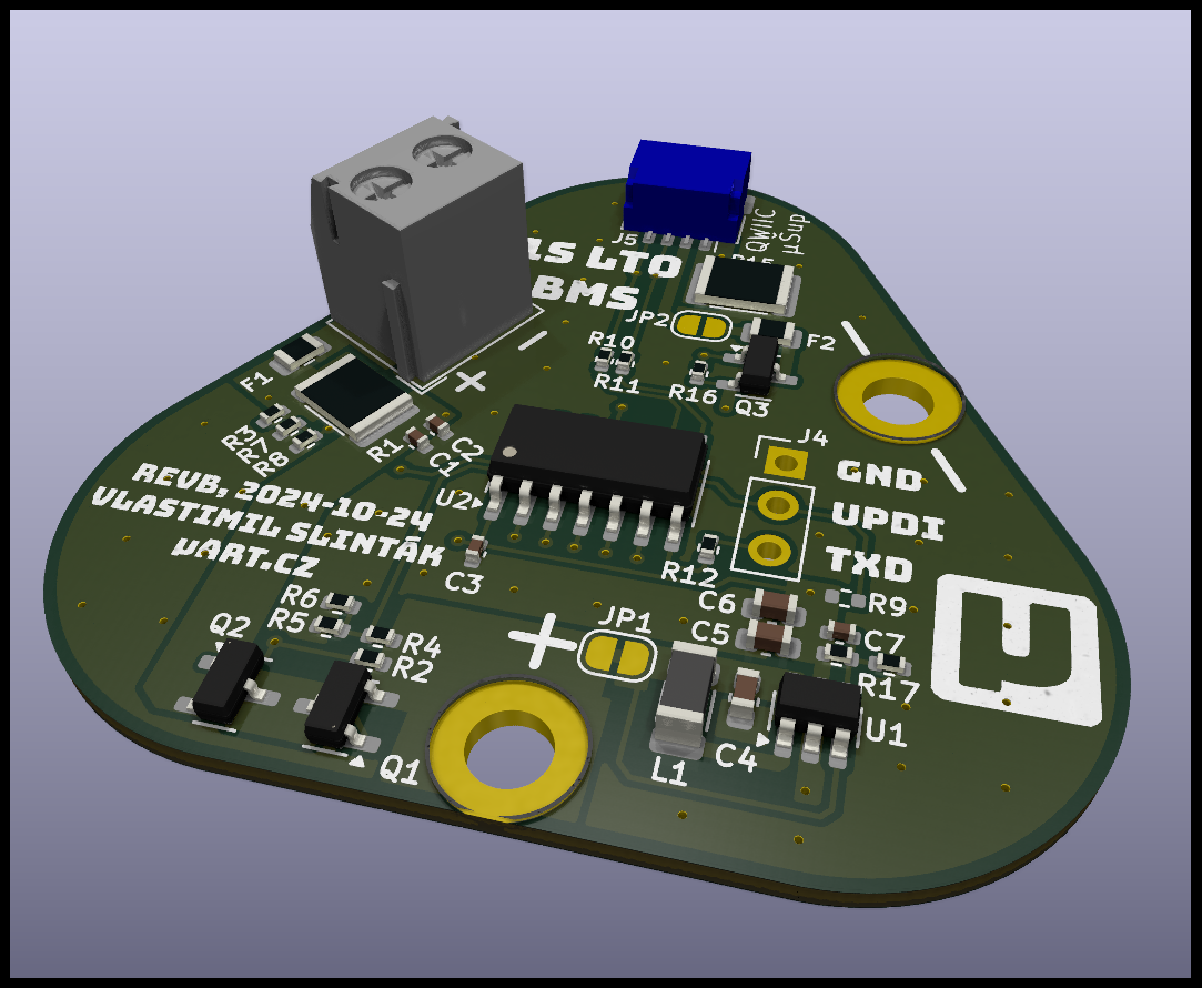
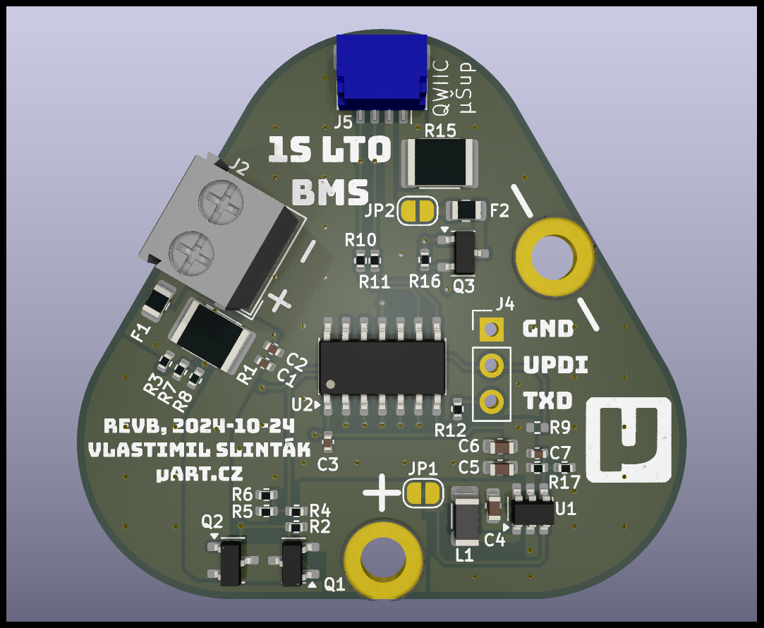
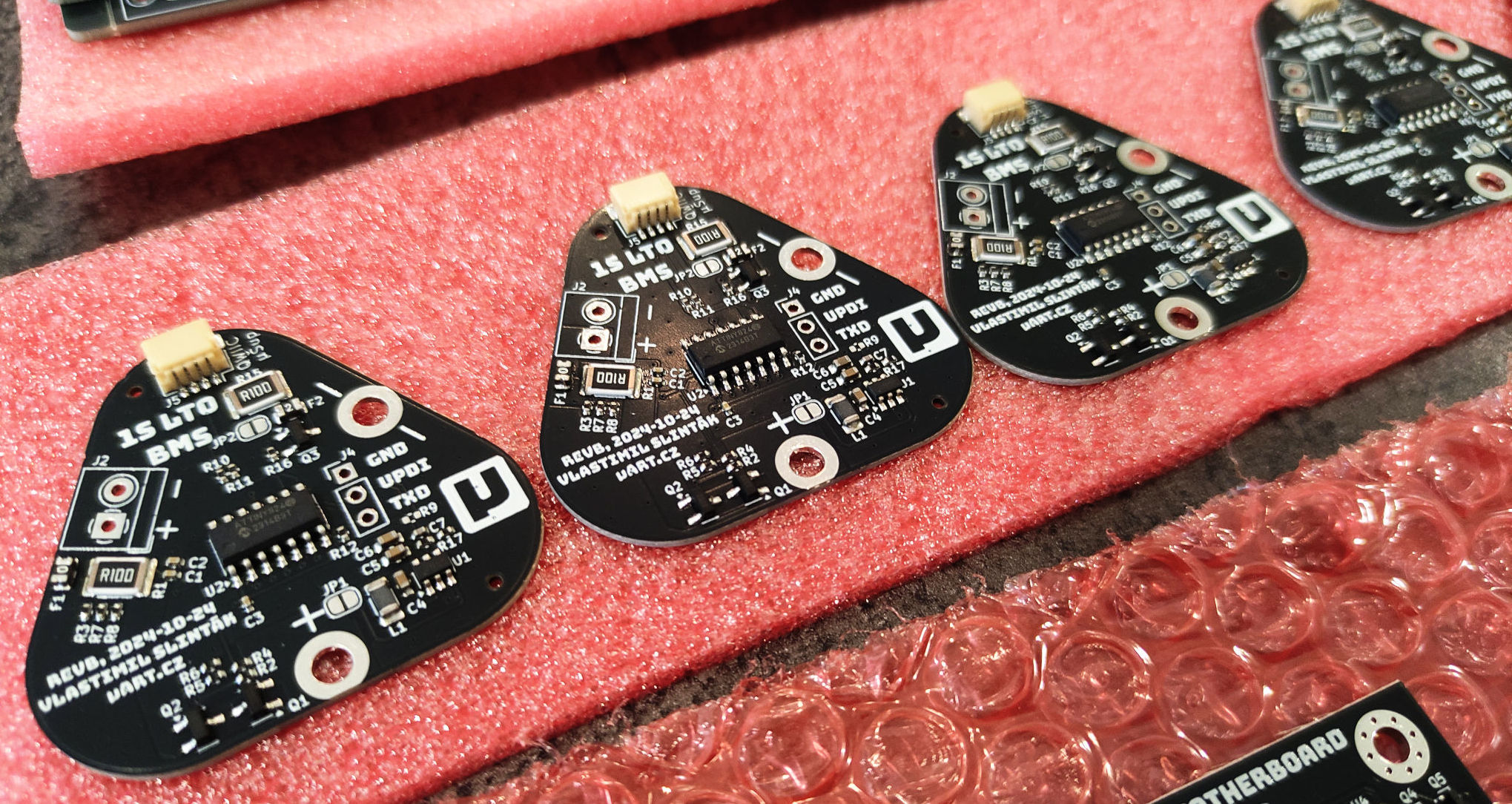
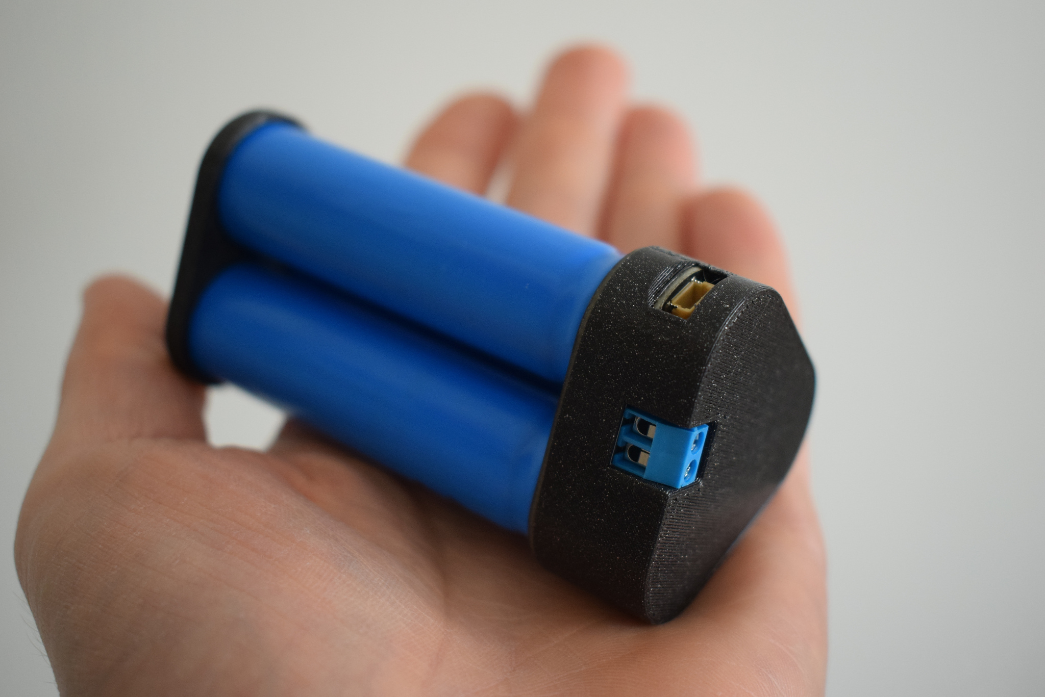
The schematic and PCB layout design was straightforward. I also designed another PCB, which I call LTO-PACK, to connect three LTO cells into a 1S3P configuration and connect them with two M3 bolts to the LTO-BMS PCB. Manufacturing and assembly were again done at JLCPCB, and within a week, everything arrived, allowing me to start coding.
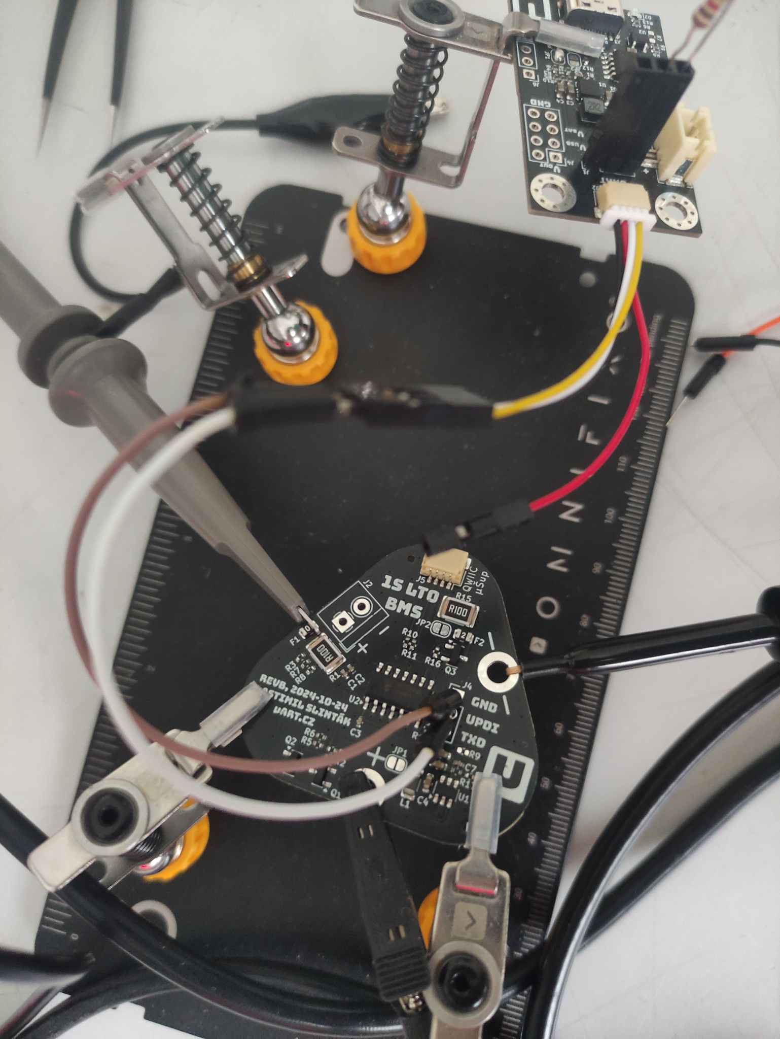
The initial version of the code, implementing OVLO, UVLO, OC, and switching the load per the configured rules, was written in about two evenings. For testing purposes, I logged all measured values every second to the UART, collected data on my PC via my USB-UART converter (also used for UPDI programming of ATTiny), and stored it in InfluxDB. A quick Grafana dashboard setup and several days of discharge/charge testing could begin.

The basic BMS functionality works. Hooray!
In the end, I implemented the I2C interface. I mimicked the INA260 registers, an integrated circuit for measuring voltage and current supported in Meshtastic firmware. Thanks to this, I was able to connect the BMS to my Meshtastic motherboard and instantly see battery voltage and discharge/charge currents in the Meshtastic app.
Sharing my partial successes on Twitter revealed significant interest in LTO and the entire BMS. Many thanks to everyone who reached out with intriguing questions and insights. It prompted me to consider several alterations I’d like to implement in the next BMS PCB revision.
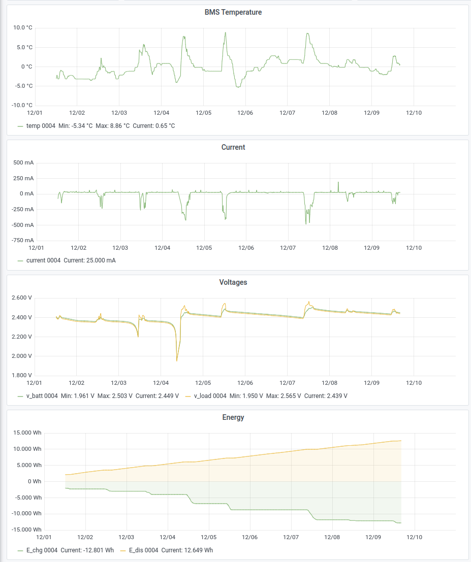
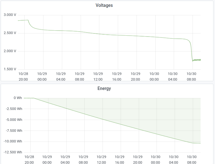
The graphs above show several days’ worth of recordings of voltage, currents, energy, and temperatures in real-world deployment on a Meshtastic station. This was in December 2024, during temperatures even below freezing, providing ideal testing conditions for LTO batteries. The firmware did not restart even once during the entire testing period and everything worked as expected. Many thanks to Zdeněk M. for his willingness and the time dedicated to collecting this test data.
Prototype No. 3
Based on my testing and others’ feedback, I’ve expanded the schematic from the previous prototype with:
- The charge pump in prototype 2 wasn’t ideal; I replaced it with a step-up converter that turns LTO voltage into a stable 3.3 V.
- I connected this stabilized voltage to the PPTC and the MOSFET transistor to the I2C connector. This allows the battery to be easily used in any application requiring 3.3 V and up to 200 mA. I hope it dramatically simplifies using LTO batteries in your projects.
- Another shunt resistor for measuring current on the stabilized 3.3 V output, allowing separate current measurement on both the unstabilized battery output and stabilized step-up converter output.
- MOSFET transistors EV3415 were replaced with SI2333, which offers better RDS(on) and is more readily available and in stock.

The new version went into production on January 7, 2025, and a week later, it was on my desk. Quite a bit of time passed from design to manufacturing; first, I was waiting for the ATtiny824 to be in stock at JLCPCB, and then I didn’t have time during the Christmas holidays. But now I have everything at home and can continue with my development.
The basic functionality remained unchanged and continues to work. The stabilized 3.3 V output on the QWIIC connector is operational, but I will still need to add support in the firmware, especially for the current measurement. Replacing the charge pump with a DC/DC converter was a very good decision. The previous consumption of the BMS itself ranged from 1-4 mA, now the standby consumption is ~55 µA. The converter is very efficient, and the MCU sleeps (standby mode) most of the time and wakes up only once per second for measurements. During this time (approximately 10 ms), the consumption increases to 1245 µA.
The table below shows the approximate circuit consumption for different supply voltages. The measurement is only approximate and will certainly change once the firmware is adjusted and fine-tuned. There are still many areas in the code that can be optimized.
| Battery Voltage | Standby Current | Measurement Current (10 ms) | Consumption |
| 2.80 V | 50 µA | 1020 µA | 60.2 µAh |
| 2.45 V | 55 µA | 1245 µA | 67.45 µAh |
| 1.80 V | 290 µA | 2242 µA | 312.42 µAh |
| 1.40 V | 235 µA | 4115 µA | 276.15 µAh |
From previous measurements (see graphs above), we know that LTO batteries have a cell voltage of approximately 2.45 V at low discharge currents, which they maintain throughout most of the discharge cycle. The voltage starts to drop sharply when the battery is almost completely discharged. Hence, we can count on an average consumption of the BMS circuit at 67.45 µAh. If we leave a 1300 mAh cell connected to the BMS without load, it will discharge in about 19,000 hours, roughly two years.
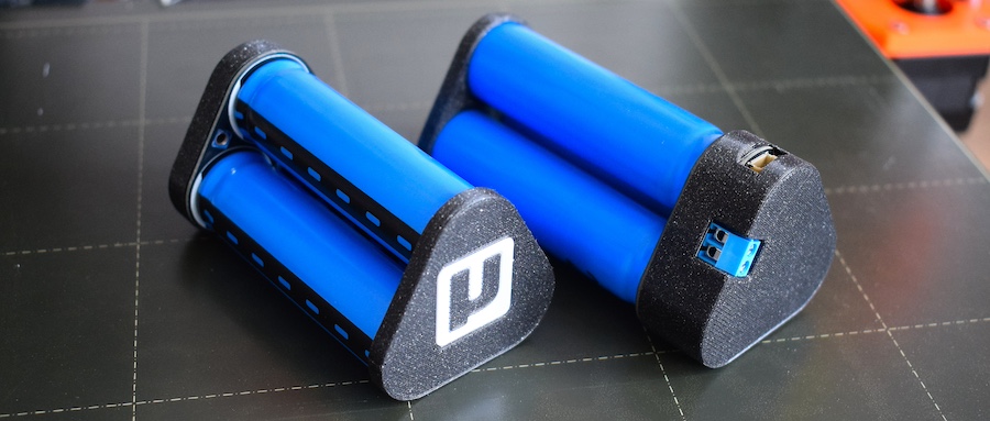
Later I was waiting for a delivery of 20 pieces of 1300 mAh LTO cells from a new manufacturer. The cells I had been using until then (the ones in all the photos) were purchased from Aliexpress, where the seller had described them as “3000 mAh LTO 25000 cycles,” which was obviously nonsense and didn’t inspire confidence. Therefore, I started looking for a better supplier so that I could produce the first larger series of complete batteries and finally equip all of my (and your) Meshtastic nodes with them.
The cells arrived, and after thorough testing, everything checked out. The capacity matched the manufacturer’s specifications, and the other parameters were also good. After several weeks of continuous charging and discharging, I ordered another 200 pieces from the same manufacturer.
These 200 cells arrived in April 2025, and I immediately began assembling the first “mass” production run of 60 battery packs. They are now available for purchase on my Lectronz store.
Detailed datasheet of the product is available: LTO Battery Pack with BMS datasheet.
Conclusion
The primary development of the PCB is now complete, and the project has entered a new phase. The firmware still requires a few minor tweaks, and I’m planning to add more metrics accessible over I2C. I’m also exploring the possibility of offering larger battery packs with 6, 9, or even 12 cells in parallel for higher capacity applications.
I’d like to thank all the volunteers who responded to my testing call at the end of 2024. Your measurements and feedback were invaluable in helping move the project forward.
As new updates come, I’ll continue to share them here. In the meantime, you can follow me on Twitter (mostly in Czech) or Bluesky (in English) for real-time progress and behind-the-scenes insights.