Who wouldn’t know GameBoy and games like Pokémon, Super Mario Land, Kirby’s Dream Land, The Legend of Zelda, etc? I grew up with these games, especially Pokémon Crystal for GameBoy Color. However, I never owned the original hardware, and later I played these games on a PC emulator.
I wanted to play Pokémon Crystal again recently, so I tried it on an Android emulator. The experience was good, just as I remembered, but I was bothered by not having real buttons and having to press the touch screen. So, I started to think how challenging it would be to create my own hardware emulating the GameBoy console.
I began searching to see if anyone had already done something similar. Some have, but not many. For example, the PicoPad development board popular here in Czechia, which you can order as a kit and is primarily focused on education. It doesn’t look like a GameBoy, and at the time when I started my design, it probably didn’t yet support GameBoy emulation (I’m not sure about this; I certainly found out about the possibility of playing GameBoy games only later). There’s also the Analogue Pocket, nice looking gaming console priced over 250 USD, unfortunately not available for shipping to the Czech Republic from their online store. However, that’s already a finished product — you buy it and play. I was missing the fun of creating something myself, spending countless hours designing electronics, tuning the emulator for a low-cost MCU, and 3D printing.
I also found DIY projects, like gb.teensy or Pico-GB. Both projects use custom hardware hacked together on a breadboard and emulator software running on a selected MCU. In the case of Pico-GB, it’s a Raspberry Pico (and therefore the RP2040 MCU).
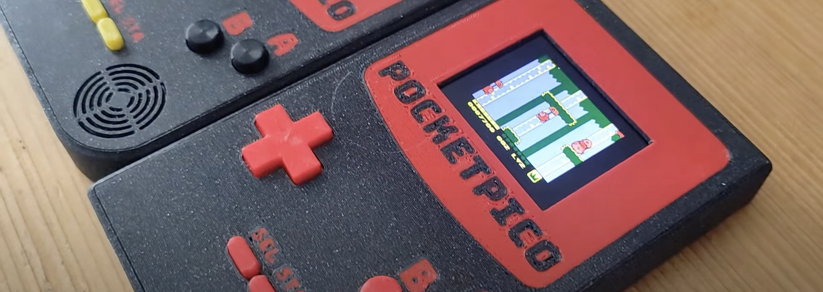
The video below shows the final version of my PocketPico, which is described in detail in the text below.
Pico-GB Project
This project caught my interest. Who isn’t familiar with the RP2040, the popular MCU from Raspberry Foundation — a dual-core 32-bit ARM Cortex-M0+ with a 133 MHz frequency, 264 kB RAM with external flash on the QSPI bus, and 30 GPIO. Plus, features like USB 1.1, PIO, DMA, good documentation, and an easy development environment pico-sdk. All of this is on a development board for about 5 EUR, or just the MCU itself in QFN-56 packaging for less than 1 EUR. I had long wanted to learn how to use this processor, but until now, there wasn’t an opportunity or an interesting project… until now.
The goals are clear:
- Build a functional GameBoy emulator (optionally GameBoy Color version) and
- learn how to use the RP2040 and pico-sdk in the process.
Prototype on a Breadboard
Let’s start with the same components used in the Pico-GB project, namely the
- ILI9225 display module with an SD card slot,
- I2S audio amplifier,
- a small 3W, 4Ohm speaker,
- Raspberry Pico,
- 8 buttons, and
- a breadboard and a few wires.
The links above are affiliate links for the Aliexpress products. If you don’t want to buy on Aliexpress, you can find most of the components locally. They are quite popular in the Arduino and Raspberry hobby stores.
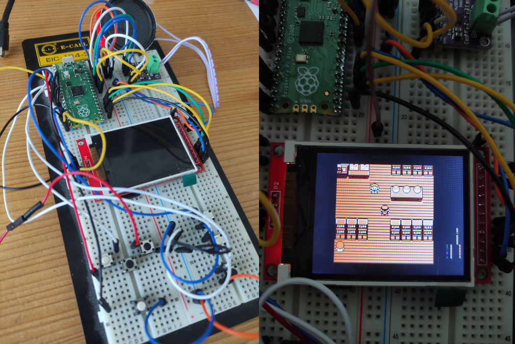
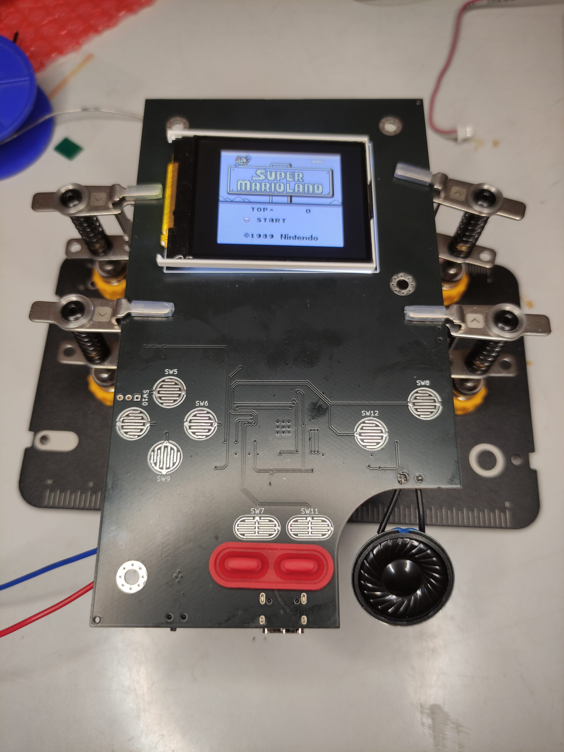
The first goal is accomplished; the GameBoy emulator is functional. However, we haven’t learned much about the RP2040, so it’s time to design our own circuit and produce a PCB.
The Raspberry Foundation has excellent documentation that describes the minimum viable circuit with the RP2040. I recommend thoroughly reviewing this document; it contains lots of useful information. With this, we can start making the schematics for our new PCB.
Designing Custom Hardware
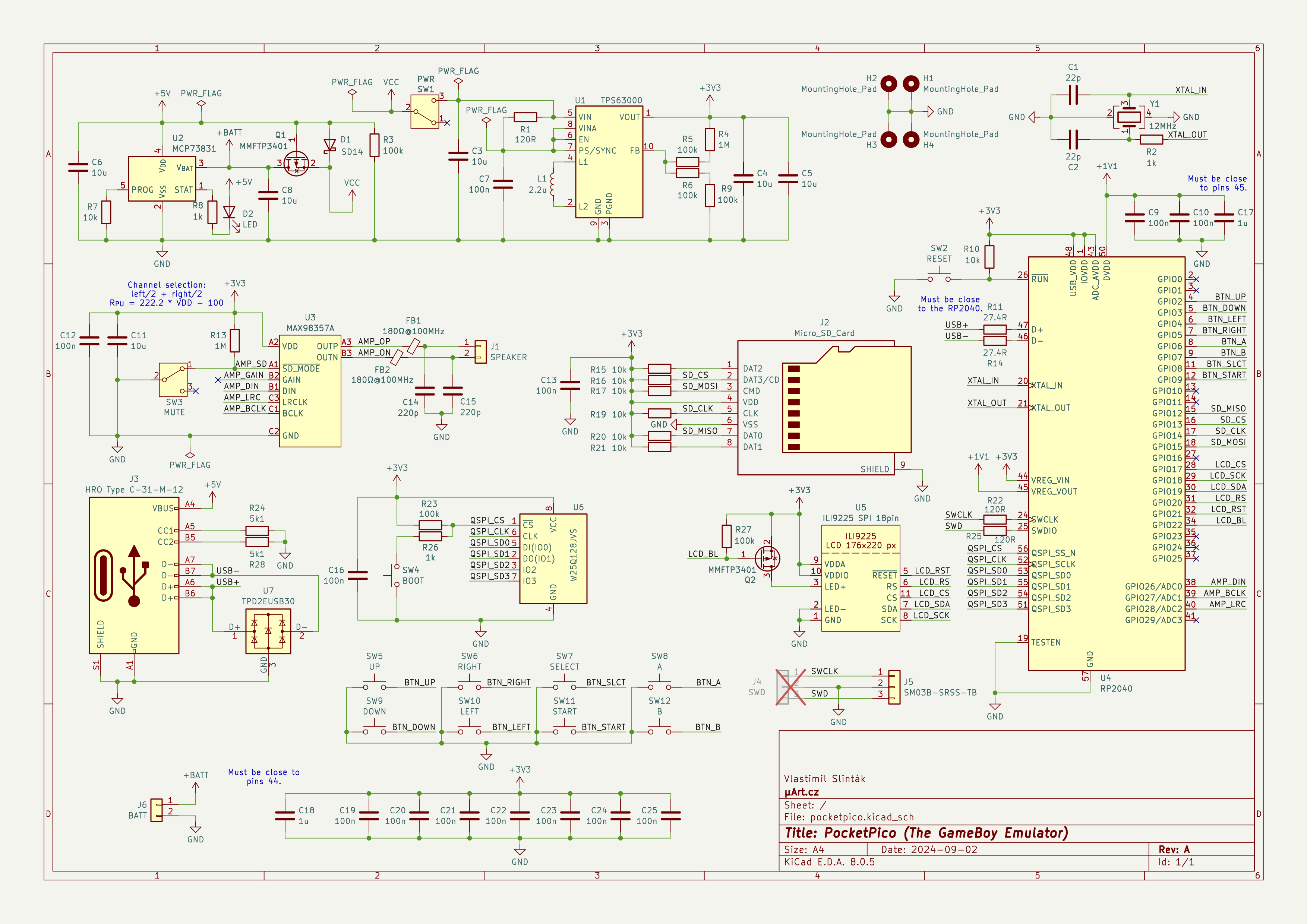
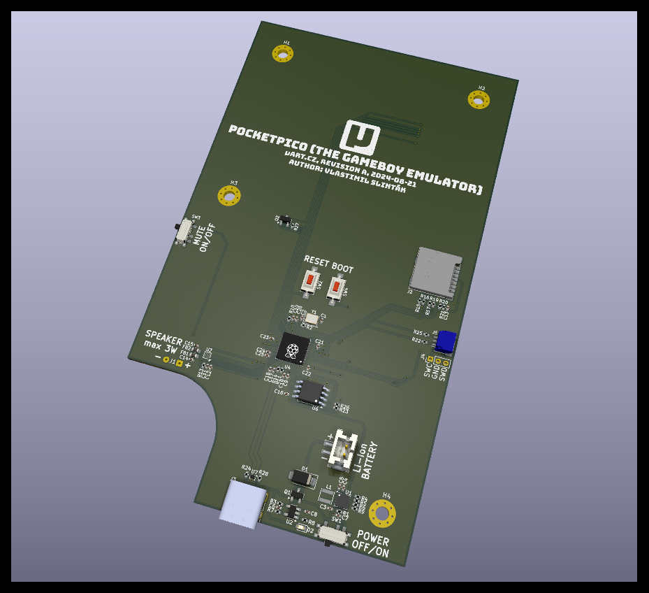
The image below shows the final schematics of my version of the GameBoy emulator, which I call PocketPico, loosely based on the Pico-GB project. I recreated the entire bird’s nest I made on a breadboard in KiCAD, but instead of using ready-made development boards and a display module, I assembled everything from individual components. I added a charger for a 1S Li-Ion battery, a buck/boost converter for stable 3.3V, and two switches for ON/OFF and sound mute. The bonus is a USB-C instead of the commonly used USB micro (typically used on the Raspberry Pico board).
Don’t worry, we’ll go through all parts of the schematics now. If you’re not interested in a detailed hardware description, feel free to skip to the next section.
Microprocessor
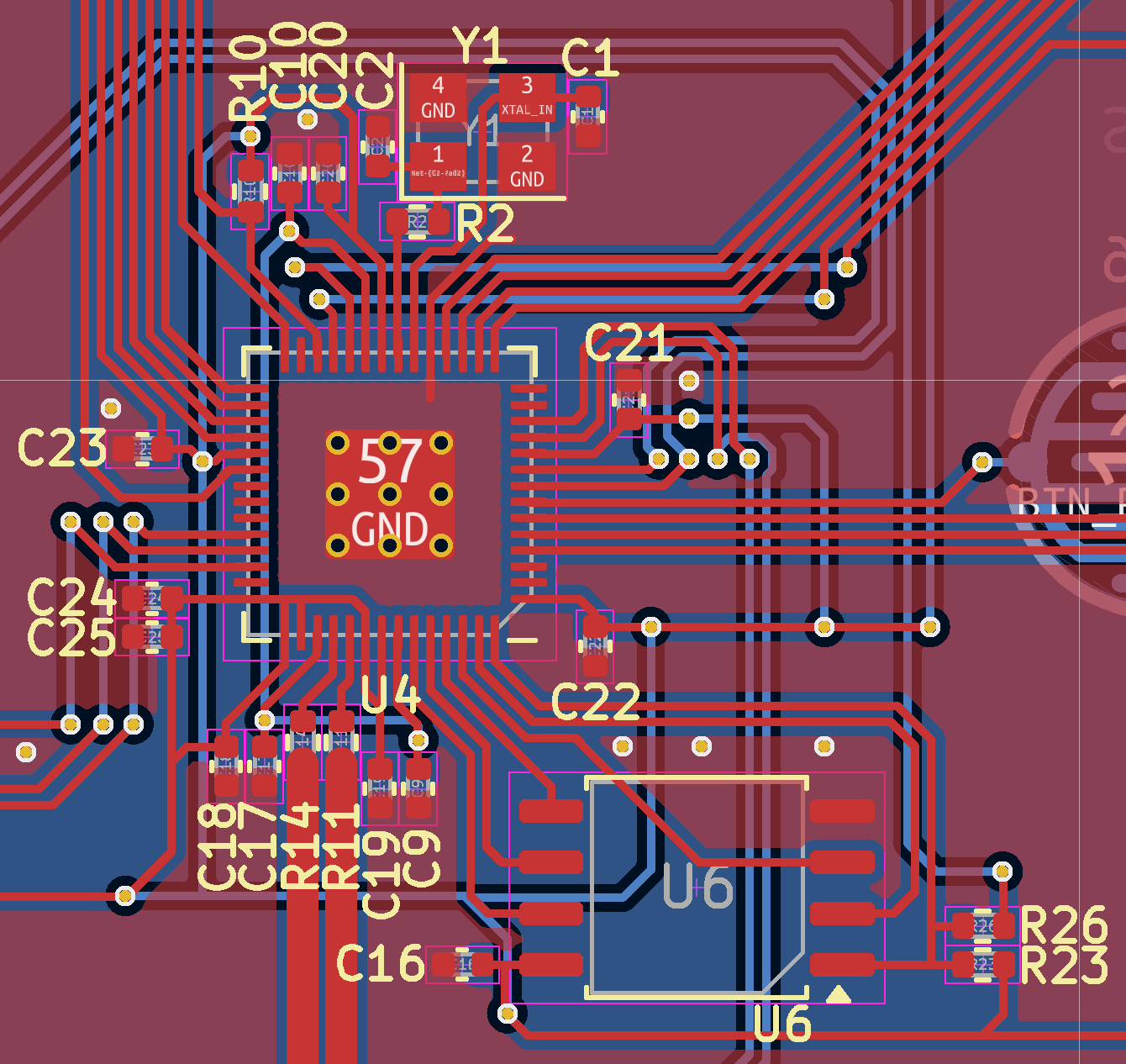
The RP2040 requires a 12 MHz crystal, and the manufacturer recommends the type ABM8-272-T3 with 15 pF capacitors to ground. I ended up using the cheaper variant X322512MSB4SI, which is readily available at JLCPCB, where I will assemble the PCBs.
Furthermore, it’s necessary to wire the FLASH memory on the QSPI bus and provide a button for the CS signal. This is used to activate the bootloader at startup, allowing new firmware to be uploaded to the MCU via USB mass storage. On Raspberry Pico boards, this button is labeled as BOOTSEL. The idea is that by holding the button and connecting the power, the user prevents the RP2040’s internal bootloader from reading data from external FLASH, which is interpreted as a signal for firmware update. This activates the USB interface, MCU announces itself on the USB as mass storage and waits for a binary file with the firmware in UF2 format. No special programmer is needed.
The RUN signal serves as the main reset for the MCU and requires a pull-up resistor. It’s also a good idea to place a button to ground on it to act as a RESET button. Together with BOOTSEL, this allows triggering a firmware update without the need to disconnect the power.
Last but not least are decoupling capacitors. One 100 nF for each VDD pin and 1 µF for each pin 44 and 45, for the internal 1.1 V regulator. This voltage must then be connected to pin 50 DVDD.
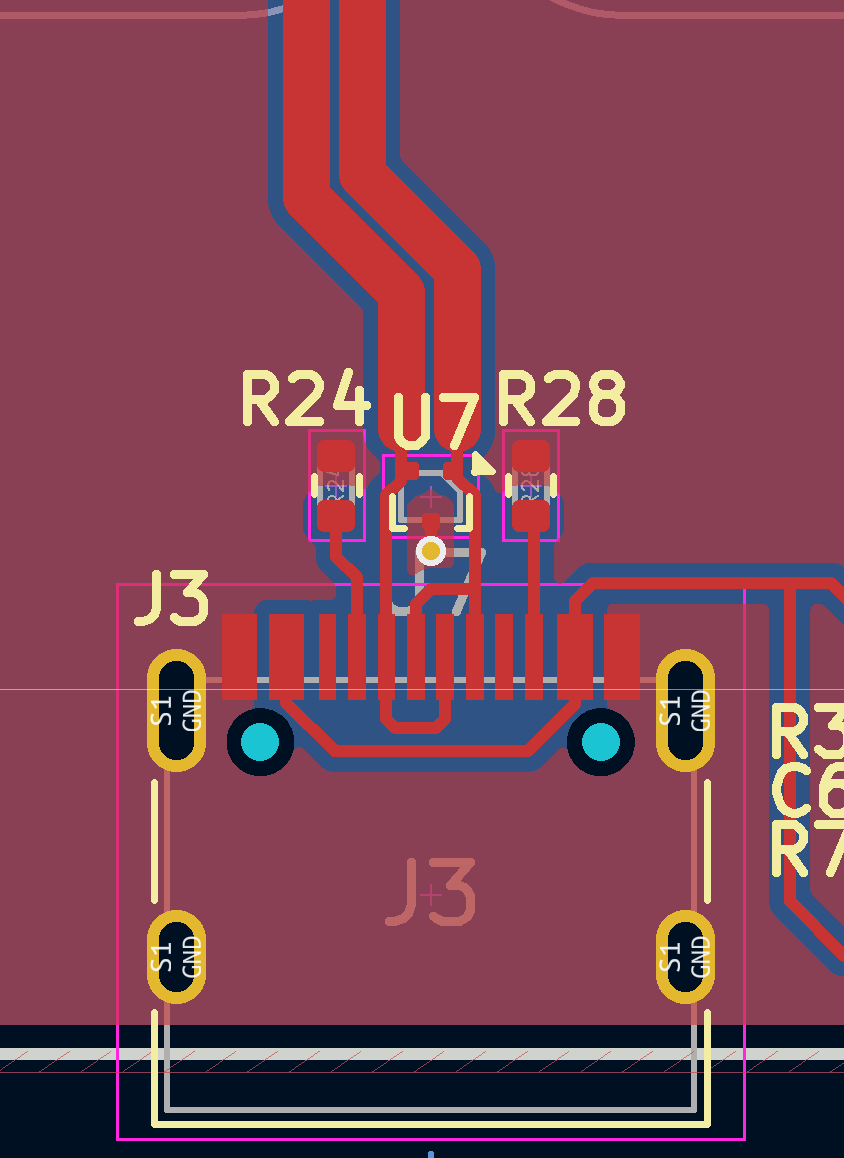
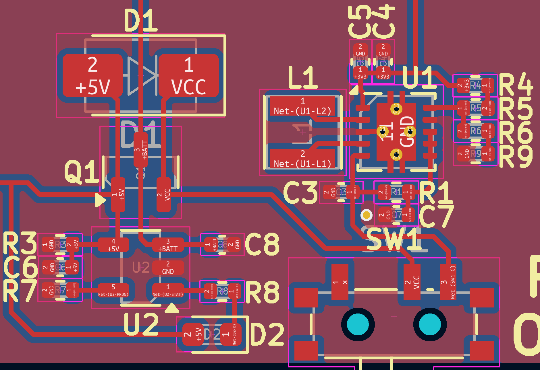
The final layout on a 2-layer PCB is shown in the image below. Notice that the decoupling capacitors are size 0402 and placed as close as possible to the MCU’s VDD pins. The crystal is also very close to the MCU, so the paths are as short as possible and do not create an unintended antenna for high-frequency signals. The last critical component is the flash memory and its QSPI bus.
USB-C
The USB-C connector has many more pins than its predecessors, and the wiring is more complex. Since we don’t need SuperSpeed USB, also known as USB 3.0, we can manage with 8 pins (SuperSpeed USB-C has 24 in total):
- VCC and GND for 5V power supply,
- 2× D+ and D- for data transfer, and
- CC1 and CC2 for configuration.
Pins CC1 and CC2 are new in USB-C and serve both sides to detect who should provide power, how much current, and other details. Our PocketPico will act as a USB device on the bus and doesn’t need any voltage other than 5V. Thus, the situation is very simple, and we need only two 5.1 kΩ resistors connected to the ground. This informs the bus master that we are a device, we require 5V and a maximum of 3A. Without these pull-down resistors, some smarter USB chargers or computers may not function correctly (practically anything with a USB-C connector on both ends won’t work).
To protect the data pins from electrostatic discharge, for example, when a user accidentally transfers static electricity to the USB connector, we use protective diodes TPD2EUSB30. These are specifically designed to protect USB data signals.
It’s worth mentioning the width of the data signals on the PCB. These signals are high-frequency on the USB bus and require an impedance of 90 Ω differentially (as specified by USB standards). This requirement is not as critical for full-speed USB 1.1 (i.e., 12 Mbps), but we should still strive to design our devices as well as possible. For 1 mm thick PCBs made from FR4 material, the path width should be 0.8 mm with a 0.15 mm gap between them, and along the entire path, there should be a complete copper plane in the bottom layer connected to the ground.
Here, I deviated a bit from the recommendations, as I don’t have an ideal ground plane under the USB signal, as seen in the layout image. I haven’t encountered any problems when using USB, but it’s something I should address and correct in the next board revision.
If higher speeds are required (a higher version of USB than 1.1), you will probably have to use a 4-layer PCB. I managed to design the PocketPico on a 2-layer board, albeit at the cost of a non-ideal ground plane.
Power Supply Section
Another important component is charging the battery using voltage from USB-C, followed by a buck/boost converter generating a stable 3.3 V for the rest of the board.
The design uses relatively low voltage and current, so there was no need for anything complicated. For the Li-Ion charging circuit, I used the MCP73831, and the DC/DC converter that stabilizes the working voltage from the battery is the TPS63000. In both cases, it’s advisable to adhere to the manufacturer’s recommended layout.
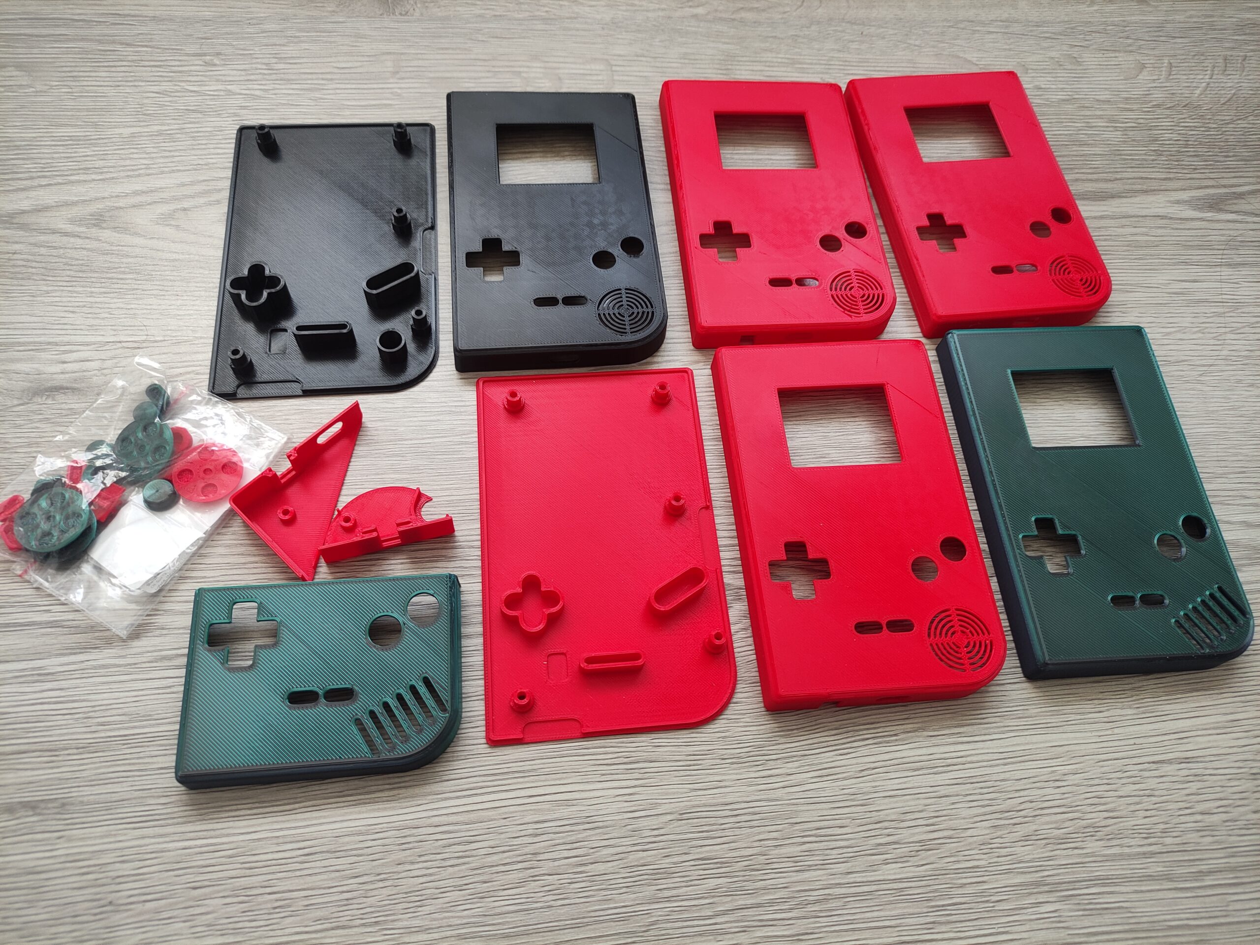
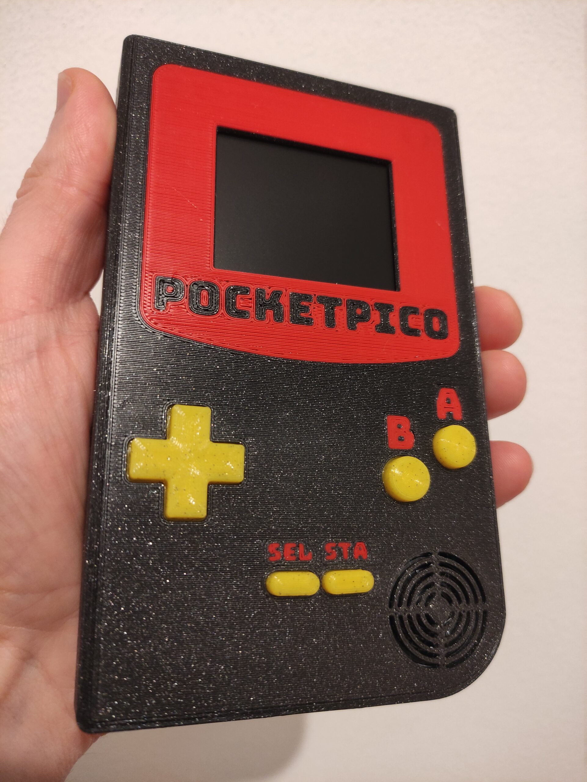
Final Result
Firmware
Peanut-GB, by author deltabeard, is a library for emulating the Game Boy console hardware (DMG) written in C99. It consists of a single file and is designed to be very fast and easily portable. This allows its use on various platforms, including our microcontroller RP2040. It supports basic Game Boy features like MBC1-MBC5, real-time clock (RTC), serial linking, and various rendering options. While it is still in development and may not be entirely accurate, it provides fast emulation. Currently, the library supports only the original Game Boy, but work is underway to support the Game Boy Color.
Peanut-GB does not support sound emulation, but this functionality can be easily added using an external library for audio processing (APU). Peanut-GB calls the functions audio_read and audio_write, which we must implement ourselves if we want sound.
The output of these functions can be sent to another library from the same author, minigb_apu. This is a fast library for emulating Game Boy sound with 16-bit output. It was designed for use on low-power microcontrollers, so it doesn’t use floating-point calculations, and some variables are fixed during the compilation time. Despite these limitations, minigb_apu is fully functional and will suffice for our purposes.
My code is based on the previously mentioned Pico-GB by YouMakeTech, which in turn is based on RP2040-GB by deltabeard, the original author of the Peanut-GB emulator. Both projects are under the MIT license, so they can be taken, modified, and published. My fork is thus available on Github as PocketPico under the MIT license.
I’ve added and modified several things in the original Pico-GB code:
- All used external libraries have been added as Git submodules. This will simplify later updates and further development.
- The audio sample rate is now 32,768 kHz instead of the original 44.1 kHz. The new value matches the audio in the original GameBoy.
- LCD control now utilizes PIO, and graphical data is sent to the LCD via DMA. This freed up one RP2040 core to do other things. This was probably the most interesting part of the project, as I had to study the functionality of PIO and learn its assembly language.
- Audio processing is now handled by the second RP2040 core.
- The project automatically compiles using Github Actions with every commit.
For now, that is all. There are many ideas for improvements, but time is in short supply. If you are interested in the project and want to contribute to its development, please contact me. I have several pieces of hardware I manufactured that I can pass on at manufacturing cost to anyone in Europe in exchange for a commitment to implement some new functionality.
What could still be improved?
- The main menu for selecting games stored on the SD card. The menu is currently very minimalistic, with a black background and white text. Some better graphics, perhaps using the LVGL library, would enhance the user experience.
- Implement a mass-storage in RP2040 to delete, add, and modify games stored on the SD card via USB. Currently, PocketPico must be disassembled, and the SD card removed if a user wants to change games.
- Improve saving the state of the running game. Currently, the game’s immediate state is saved by writing to a file on the SD card. It would be nice to be able to save multiple states of the same game and then have a menu to load previous states.
- Support for Game Boy Color games! I would love to play Pokémon Crystal.
- Anything else.
Now that we’ve covered the PocketPico firmware introduction, let’s look at perhaps the most interesting component of the RP2040 chip – PIO. In PocketPico, it’s used for the I2S bus to send digital audio signals to the amplifier. Later, I used PIO to generate a VGA signal from PocketPico to a display with a resolution of 480×480 pixels (this was just an experiment that isn’t part of the published code yet). As the goal of this project is to learn with the RP2040, I will describe the functioning principle of PIO in more detail.
Programmable Input/Output
Unlike other microcontrollers, the RP2040 doesn’t have many peripherals available. There are only USB, UART, I2C, SPI, and PWM. If you need anything else (e.g., CAN bus, I2S, 1-Wire, WS2812, VGA, …), you must use one of the two available “programmable input/output blocks”. PIO is a powerful tool that allows the implementation of almost any interface, but it requires thorough documentation study and a bit of low-level programming.
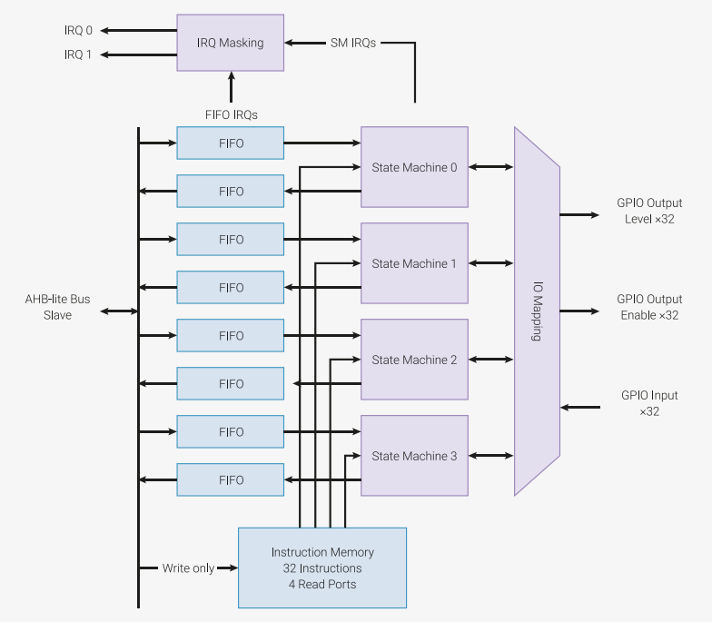
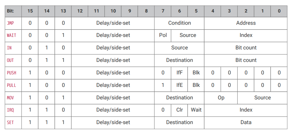
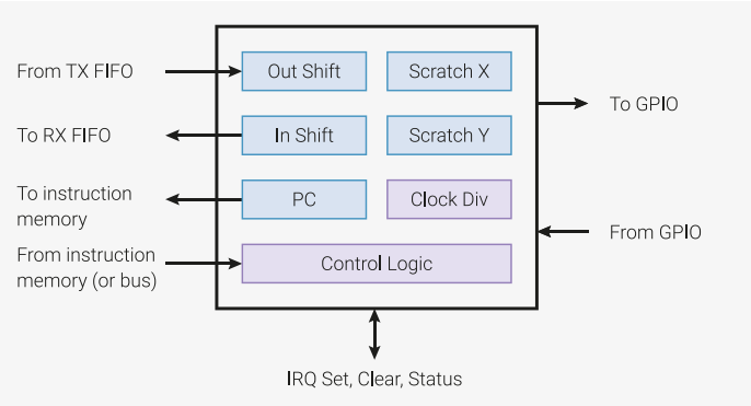
Imagine a PIO block as four miniature and very simple processors with a shared memory of 32 instructions. Each PIO “processor” (referred to as “state machines” in the RP2040 datasheet) has two FIFO queues for input and output data to/from the main processor and can control any number of GPIO pins. Programming PIO uses an assembly language that has nine instructions.
Does nine available instructions and program memory for 32 instructions seem limited? Remember, PIO is designed to control GPIO pins and transfer data between the outside world and RP2040 memory, all without needing the main processor. PIO is designed for this purpose, and the available resources are usually sufficient.
A program written in C and running on the RP2040’s main processor must first configure PIO, upload instructions to PIO memory, set which GPIO pins will be “out” and “side set”, and determine at what speed the PIO code will execute. This is done using the following functions (there are actually more, the following block contains just a few examples):
sm_config_set_out_pins();
sm_config_set_sideset_pins();
sm_config_set_clkdiv();
pio_sm_init();
pio_sm_set_enabled();
Each PIO has four independent state machines (SM) and can have four independent programs with different GPIOs and settings. Programs are always stored in one shared memory of 32 instructions, but each SM has its own input and output FIFO queues, which serve to pass data between main memory and SM PIO.
If we want to send data to a specific SM PIO from the main C program, we simply call the function pio_sm_put_blocking(pio, sm, (uint32_t)c). This takes a 32-bit number in the variable c and puts it into the RX FIFO queue of the state machine sm in PIO number pio. Reading 32-bit numbers from SM PIO is similar. Both queues (RX and TX) are 4×32 bits in size. If we know one queue won’t be needed in SM PIO (for example, if we only store data in SM and never read), both queues can be combined into one 8×32-bit FIFO for one direction.
Besides instruction memory and FIFO queues, each SM PIO also has two 32-bit registers, X and Y, called “scratch registers” in the documentation, and shift registers OSR (output shift register) and ISR (input shift register).
Each instruction (and all its side effects) executes in a single clock cycle. This means if you need to generate a square wave signal at 1 MHz, you must divide the processor’s clock signal (which is 133 MHz usually) by 66.5 to get a 2 MHz clock signal for SM. The program will then contain two instructions that alternately set HIGH and LOW on the output GPIO pin, giving you a 1 MHz signal. The SM clock generator supports non-integer values, so almost any frequency is possible.
PIO instructions have several side functions aside from their main purpose. It can control one or more pins (called “side set” in the documentation, defined outside the PIO program using the aforementioned sm_config_set_sideset_pins() function) simultaneously with the main function of the instruction. For example, the `pull` instruction loads a 32-bit word from the TX FIFO queue. If the keyword `side` is included, all side set pins are set to a HIGH or LOW level, and if there’s a number in square brackets on the line, the program will halt for that many clock cycles, allowing short “delays”.
For complete documentation, I refer you to the RP2040 datasheet, the Pico C/C++ SDK, and official examples. But to give you a better idea, here’s a simple PIO program implementing TX UART, or sending 8 bits serially.
.program uart_tx
.side_set 1 opt
    pull       side 1 [7]
    set x, 7   side 0 [7]
bitloop:
    out pins, 1
    jmp x-- bitloop   [6]
This code will be in the uart_tx.pio file along with several other functions in C. The complete example is available in the pico-examples repository.
Take another look at the example code and notice that some keywords start with a dot, some lines contain just a string and a colon, and some lines contain “instruction”, its parameters, the keyword “side”, and a number in square brackets. What does this all mean?
Words starting with a dot are program directives, which don’t execute any function in the PIO program but only set the PIO assembler. For example, .program tell the assembler what is the name of the following program. During compilation, the assembler generates an interface for the C language and uses this name in function names. The .side_set directive sets the number of side set pins. Lines with a string ending with a colon are called labels, which just mark a specific line with a human-readable name. This name can then be referred to in the program (look at the last line with the jmp instruction, where the label bitloop is used).
The sample program functions as follows:
- `pull`: The instruction takes one word (32 bits) from the RX FIFO queue and stores it in the OSR register. Simultaneously, the side pin is set to logical 1. The program then waits (halts) for exactly 7 clock cycles.
- `set`: The constant 7 is stored in the X register, the side pin is set to logical 0, and then it waits for 7 clock cycles.
- `out`: The MSB (least significant bit) value from the OSR register is sent to the output pin.
- `jmp`: The register value is decremented by 1, and it waits for 6 clock cycles. It then either continues from the beginning of the program (if
X == 0) or jumps to the labelbitloopand continues from there.
I recommend you to look at the whole example and also focus on the C functions used to configure PIO and SM.
Here’s a code using one SM in one PIO implementing I2S. This code is used in PocketPico to send audio data to the digital amplifier MAX98357A.
.program audio_i2s
.side_set 2
                    ;        /--- LRCLK
                    ;        |/-- BCLK
bitloop1:           ;        ||
    out pins, 1       side 0b10
    jmp x-- bitloop1  side 0b11
    out pins, 1       side 0b00
    set x, 14         side 0b01

bitloop0:
    out pins, 1       side 0b00
    jmp x-- bitloop0  side 0b01
    out pins, 1       side 0b10
public entry_point:
    set x, 14         side 0b11
And this concludes the crash course on PIO. The information above serves as a very light introduction to PIO in RP2040, so I recommend starting with the datasheet and available examples. Don’t be discouraged at the beginning by the complexity and the number of abbreviations used. It took me one full weekend of study and experiments to start writing my own programs.
RP2350 and a Larger Display
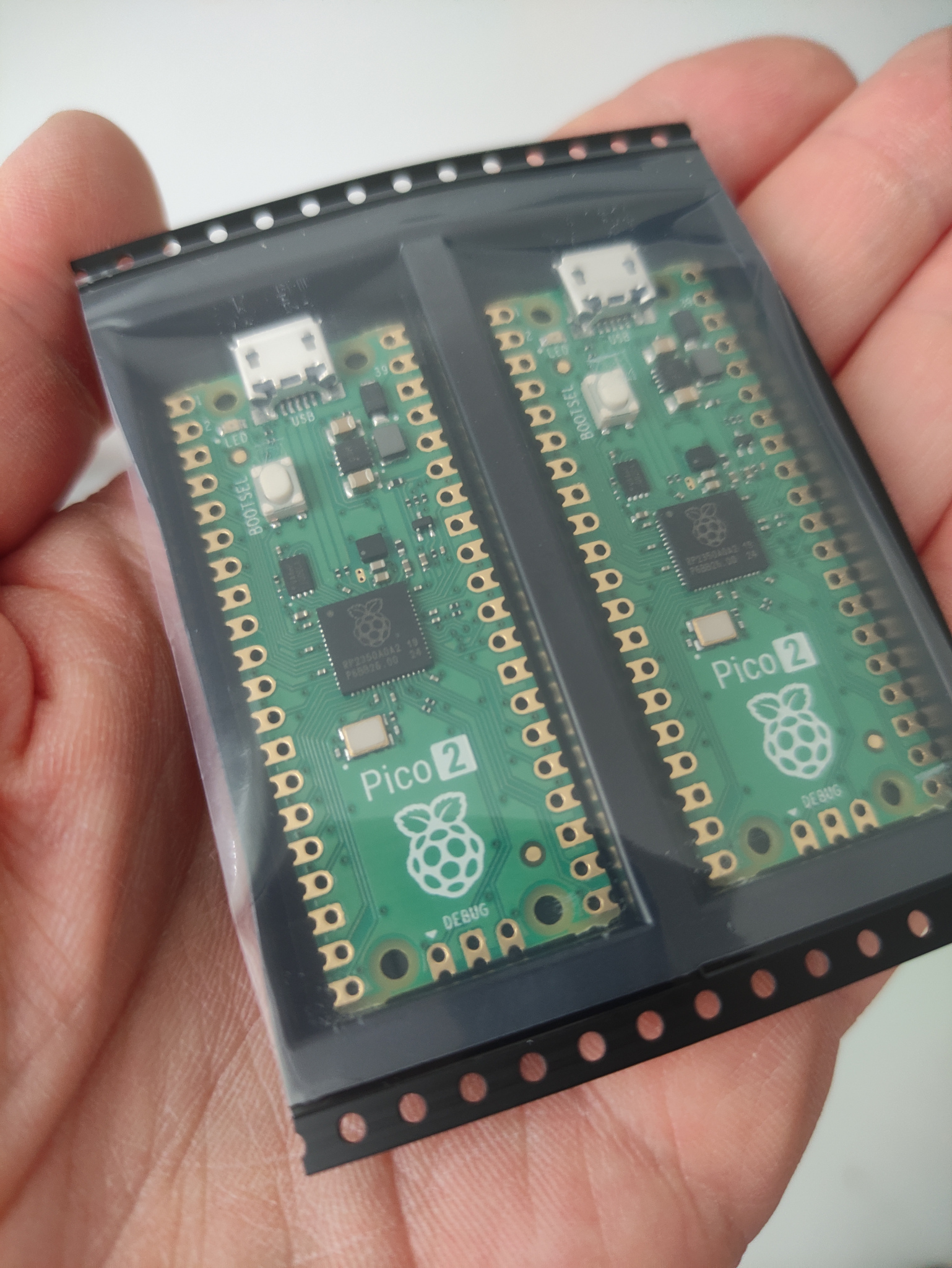
You may have noticed that the Raspberry Foundation has released a new version of the Raspberry Pico 2 with the RP2350 microcontroller. This is an enhanced version of the original RP2040. Currently, this MCU is not available standalone but only as part of the Pico2 board (although some major manufacturers already have the RP2350 and are beginning to manufacture their products).
After completing PocketPico, I ordered two Pico2 boards along with a larger LCD with a resolution of 480×480 pixels and a VGA interface. Over time, I would like to enhance PocketPico with this new MCU and the large display, but for now, I have only written a PIO program for generating a VGA signal to the display.
This PIO program uses 4 state machines of one PIO and takes up 29 instructions. Data are sent to the PIO using DMA, and the clock signal operates at a frequency of 30 MHz. From this, a pixel clock with a speed of 15 MHz is generated, providing exactly 60 Hz vertical frequency and 30 kHz horizontal at a resolution of 480×480 px (plus front and back porch, sync pulse, and other necessities in the VGA signal).
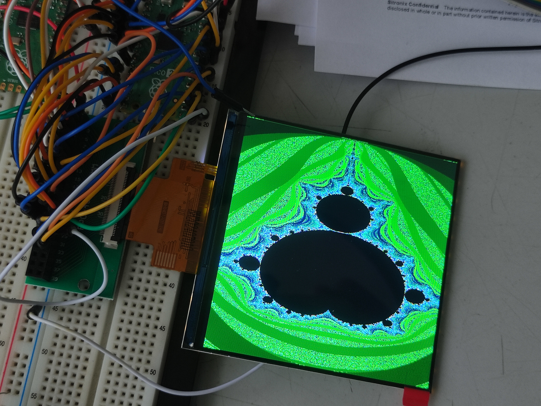
If I find the time and motivation, I plan to create a PocketPico2 with the RP2350 and this larger display. GameBoy games will then be displayed enlarged, with each original pixel becoming 3×3 pixels on the new display.
Conclusion and What’s Next?
PocketPico was showcased and available to play at the Brno MakerFaire. The console was a big hit among children and adult visitors, and I thank you all for your positive comments and interest in the games.
I have released the source code for PocketPico under the MIT license. The hardware design is not yet public, as I want to first create a new revision of the PCB (and resolve a few minor issues) and test the larger display. Once complete, I will update this text with the links.